
SMT Surface-Mount Technology Small Boards: A Comprehensive G

Abstract
SMT patch small boards (surface-mount studs/nuts), as board-level fasteners, can be directly soldered onto PCB pads using standard reflow soldering. Compared with riveting or insertion‑type soldering, their primary advantage is that they can be mounted in conjunction with component placement during SMT assembly, eliminating the need for secondary processing, and they are well suited for thin boards (with a minimum thickness of 1.0 mm) and single‑sided designs. This paper provides a systematic analysis focusing on product structure, pad design, reflow soldering processes, and common failure‑mitigation strategies.
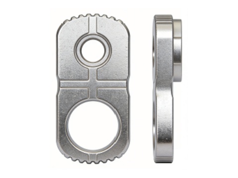
Product Structural Features
SMT surface-mount subassemblies typically consist of a threaded working portion, a flanged base, knurling, and an optional locating step. The flanged base provides shear‑/pull‑out bearing area against the PCB pads; the knurling complies with GB/T 6403.3‑2008, increasing fastening friction and creating mechanical interlocking. To ensure mounting accuracy, component coplanarity must be controlled to ≤0.10 mm; otherwise, cold solder joints or tombstoning may occur.
Pad Design Principles
Pad design is central to determining the reliability of SMT surface-mount fasteners. The recommended design principles are as follows:
·Dimensional Matching: The pad outer diameter is typically 1.2 to 1.5 mm larger than the flange outer diameter to ensure complete fillet formation by the solder.
-Positioning hole design: The hole diameter should be 0.05–0.10 mm larger than the step diameter, balancing positioning accuracy with gas venting during reflow soldering.
- Layout requirements: The distance from the pad edge must be ≥1.5 mm to prevent copper foil delamination caused by thermal stress.
Key Points of Reflow Soldering Process
SMT surface-mount boards must undergo the reflow profile alongside other components on the PCB. When using SAC305 lead-free solder paste, the recommended process window is: a preheating rate of 1.5–3.0°C/s in the preheat zone, and a soak temperature of 150–200°C maintained in the soak zone.
60–120 s; the peak temperature in the reflow zone is controlled at 245–260°C, with the time above the liquidus (TAL) maintained at 60–90 s; in the cooling zone, the cooling rate is ≤4°C/s to prevent PCB warpage and pad delamination. The fastener coating must remain solderable and non‑oxidized within this process window.
Material and Coating
Common material combinations include: carbon steel/machinable steel with tin plating (low cost, good solderability, suitable for general electronic devices); copper alloy with tin plating (excellent electrical and thermal conductivity, ideal for high-current terminals); and 300-series stainless steel with either bare or tin plating (good corrosion resistance, appropriate for medical and outdoor equipment). The solderability of the coating can be assessed using the wetting balance test specified in IPC/JEDEC J‑STD‑002; after reflow, the intermetallic compound (IMC) layer—Cu₆Sn₅/Ni₃Sn₄—should ideally be maintained at a thickness of 1–3 μm.
Common Failures and Countermeasures
In actual production, small SMT‑mounted circuit boards may face the following failure risks and corresponding mitigation strategies:
- Pad misalignment/offset: Often caused by asymmetric pads, uneven solder paste volume, or component placement deviation. Countermeasures include optimizing pad symmetry, improving component coplanarity, and recalibrating the pick‑and‑place nozzle.
- Solder bridging/voids: Typically caused by stencil apertures that are too small, solder paste slump, or insufficient temperature. It is recommended to increase the stencil area ratio, verify the solder paste’s activity, or raise the peak temperature.
- Pad delamination: This is associated with insufficient PCB thermal resistance, excessively rapid cooling, or overly thin board thickness. Consider using high‑Tg materials, reducing the cooling rate, and increasing the pad edge clearance.
- Thread pull-out: Caused by a small flange diameter or insufficient weld pad area. Increase the flange/pad size, or add locating holes/steps.
Selection Recommendations
When selecting components for an SMT‑mounted small circuit board, engineers are advised to follow these core steps:
1.Specify the thread specifications and the final tightening torque, and verify the PCB thickness, number of layers, and pad copper thickness.
2.Evaluate whether positioning steps or metallized vias are required, and determine the reflow soldering peak temperature and cycle count.
3. Select the material and coating based on the application scenario (e.g., carbon steel with tin plating, copper alloy with tin plating, or stainless steel).
4. Require suppliers to provide welding thrust, pull-off torque, coplanarity, and X-ray inspection reports, and confirm the compatibility of carrier tape packaging with the feeder.
Conclusion
SMT surface-mount circuit boards convert mechanical connection points into components that can be automatically mounted, with reliability heavily dependent on the coordinated optimization of pad design, reflow profiles, and test validation. With proper process control and component selection, it is possible to effectively meet
Meeting the high‑throughput and low‑cost requirements of consumer electronics, medical devices, telecommunications, and other applications. Yingfeng Zhicheng Jia has integrated SMT component‑placement and soldering performance testing into its technical services, offering end-to‑end support across the entire product lifecycle—from design consulting and rapid prototyping to process optimization.
References
- zcjtech.com/ SMT Chip Nut – Surface-Mount Fastener Product Page
- Yingfeng Zhicheng Jia SMT Series Catalog (SMT Slide Lock / Spring Lock / Floating Nut)
- Yingfeng Zhicheng Jia Company Introduction 2026 & Internal Training Materials for Application Engineers
- GB/T 6403.3-2008 “Knurling”
- IPC/JEDEC J-STD-002 “Solderability Test for Component Leads, Terminals, Solder Tabs, Terminal Posts, and Wires”
More Blog
- SMT Surface-Mount Technology Small Boards
- Type 308 Self-Tapping Insert: One-Shot Hi
- How Cold Heading Slashed EV Battery Lifti
- ZT68 600MPa Cold-Headed High-Strength Alu
- ZT68 600MPa Cold-Formed High-Strength Alu
- Precision Crafting for a Lightweight Futu
- Yingfeng Zhichengjia Newly Customized Spr
- R&D of ultra-high strength aluminum a